- 您现在的位置:买卖IC网 > Sheet目录1905 > ATMEGA48PA-MMNR (Atmel)MCU AVR 4KB FLASH 20MHZ 28QFN
108
8161D–AVR–10/09
ATmega48PA/88PA/168PA/328P
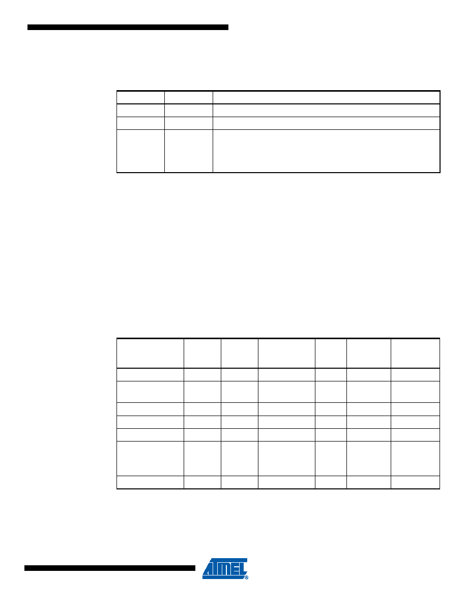
Table 14-7 shows the COM0B1:0 bit functionality when the WGM02:0 bits are set to phase cor-
rect PWM mode.
Note:
1. A special case occurs when OCR0B equals TOP and COM0B1 is set. In this case, the Com-
pare Match is ignored, but the set or clear is done at TOP. See ”Phase Correct PWM Mode” on
page 102 for more details.
Bits 3, 2 – Res: Reserved Bits
These bits are reserved bits in the ATmega48PA/88PA/168PA/328P and will always read as
zero.
Bits 1:0 – WGM01:0: Waveform Generation Mode
Combined with the WGM02 bit found in the TCCR0B Register, these bits control the counting
sequence of the counter, the source for maximum (TOP) counter value, and what type of wave-
form generation to be used, see Table 14-8. Modes of operation supported by the Timer/Counter
unit are: Normal mode (counter), Clear Timer on Compare Match (CTC) mode, and two types of
Pulse Width Modulation (PWM) modes (see ”Modes of Operation” on page 99).
Notes:
1. MAX
= 0xFF
2. BOTTOM = 0x00
Table 14-7.
Compare Output Mode, Phase Correct PWM Mode(1)
COM0B1
COM0B0
Description
0
Normal port operation, OC0B disconnected.
01
Reserved
10
Clear OC0B on Compare Match when up-counting. Set OC0B on
Compare Match when down-counting.
11
Set OC0B on Compare Match when up-counting. Clear OC0B on
Compare Match when down-counting.
Table 14-8.
Waveform Generation Mode Bit Description
Mode
WGM02
WGM01
WGM00
Timer/Counter
Mode of
Operation
TOP
Update of
OCRx at
TOV Flag
Set on
0
Normal
0xFF
Immediate
MAX
10
0
1
PWM, Phase
Correct
0xFF
TOP
BOTTOM
2
0
1
0
CTC
OCRA
Immediate
MAX
3
0
1
Fast PWM
0xFF
BOTTOM
MAX
4
1
0
Reserved
–
51
0
1
PWM, Phase
Correct
OCRA
TOP
BOTTOM
6
1
0
Reserved
–
71
1
Fast PWM
OCRA
BOTTOM
TOP
发布紧急采购,3分钟左右您将得到回复。
相关PDF资料
ATMEGA644P-B15MZ
IC MCU 8BIT 64KB FLASH 32VQFN
ATMEGA644V-10PU
IC AVR MCU FLASH 64K 40DIP
ATMEGA645V-8MI
IC AVR MCU FLASH 64K 1.8V 64QFN
ATMEGA649-16MI
IC AVR MCU FLASH 64K 5V 64QFN
ATMEGA649V-8MI
IC AVR MCU FLASH 64K 1.8V 64QFN
ATMEGA8515L-8JUR
MCU AVR 8KB FLASH 8MHZ 44PLCC
ATMEGA8515L-8PJ
IC MCU AVR 8K 5V 8MHZ 40-DIP
ATMEGA8535-16JUR
MCU AVR 8K FLASH 16MHZ 44PLCC
相关代理商/技术参数
ATMEGA48PA-MN
功能描述:8位微控制器 -MCU AVR 4KB FL 256B EE 512B SRAM 20MHz 105C RoHS:否 制造商:Silicon Labs 核心:8051 处理器系列:C8051F39x 数据总线宽度:8 bit 最大时钟频率:50 MHz 程序存储器大小:16 KB 数据 RAM 大小:1 KB 片上 ADC:Yes 工作电源电压:1.8 V to 3.6 V 工作温度范围:- 40 C to + 105 C 封装 / 箱体:QFN-20 安装风格:SMD/SMT
ATMEGA48PA-MNR
功能描述:8位微控制器 -MCU AVR 4KB FL 256B EE 512B SRAM 20MHz 105C RoHS:否 制造商:Silicon Labs 核心:8051 处理器系列:C8051F39x 数据总线宽度:8 bit 最大时钟频率:50 MHz 程序存储器大小:16 KB 数据 RAM 大小:1 KB 片上 ADC:Yes 工作电源电压:1.8 V to 3.6 V 工作温度范围:- 40 C to + 105 C 封装 / 箱体:QFN-20 安装风格:SMD/SMT
ATMEGA48PA-MU
功能描述:8位微控制器 -MCU AVR 4KB FLASH 20 MHZ,IND TEMP RoHS:否 制造商:Silicon Labs 核心:8051 处理器系列:C8051F39x 数据总线宽度:8 bit 最大时钟频率:50 MHz 程序存储器大小:16 KB 数据 RAM 大小:1 KB 片上 ADC:Yes 工作电源电压:1.8 V to 3.6 V 工作温度范围:- 40 C to + 105 C 封装 / 箱体:QFN-20 安装风格:SMD/SMT
ATMEGA48PA-MU@SL383
制造商:Atmel 功能描述:MCU 8-bit ATmega AVR RISC 4KB Flash 2.5V/3.3V/5V 32-Pin QFN EP T/R
ATMEGA48PA-MUR
功能描述:8位微控制器 -MCU AVR 4KB FLSH 256B EE 512B SRAM-20MHz IND RoHS:否 制造商:Silicon Labs 核心:8051 处理器系列:C8051F39x 数据总线宽度:8 bit 最大时钟频率:50 MHz 程序存储器大小:16 KB 数据 RAM 大小:1 KB 片上 ADC:Yes 工作电源电压:1.8 V to 3.6 V 工作温度范围:- 40 C to + 105 C 封装 / 箱体:QFN-20 安装风格:SMD/SMT
ATMEGA48PA-PN
功能描述:8位微控制器 -MCU AVR 4KB FL 256B EE 512B SRAM 20MHz 105C RoHS:否 制造商:Silicon Labs 核心:8051 处理器系列:C8051F39x 数据总线宽度:8 bit 最大时钟频率:50 MHz 程序存储器大小:16 KB 数据 RAM 大小:1 KB 片上 ADC:Yes 工作电源电压:1.8 V to 3.6 V 工作温度范围:- 40 C to + 105 C 封装 / 箱体:QFN-20 安装风格:SMD/SMT
ATMEGA48PA-PU
功能描述:8位微控制器 -MCU AVR 4KB FLASH 20 MHZ,IND TEMP RoHS:否 制造商:Silicon Labs 核心:8051 处理器系列:C8051F39x 数据总线宽度:8 bit 最大时钟频率:50 MHz 程序存储器大小:16 KB 数据 RAM 大小:1 KB 片上 ADC:Yes 工作电源电压:1.8 V to 3.6 V 工作温度范围:- 40 C to + 105 C 封装 / 箱体:QFN-20 安装风格:SMD/SMT
ATMEGA48PB-AN
功能描述:AVR AVR? ATmega Microcontroller IC 8-Bit 20MHz 4KB (2K x 16) FLASH 32-TQFP 制造商:atmel 系列:AVR? ATmega 包装:托盘 零件状态:有效 核心处理器:AVR 核心尺寸:8-位 速度:20MHz 连接性:I2C,SPI,UART/USART 外设:欠压检测/复位,POR,PWM,WDT I/O 数:27 程序存储容量:4KB(2K x 16) 程序存储器类型:闪存 EEPROM 容量:256 x 8 RAM 容量:512 x 8 电压 - 电源(Vcc/Vdd):1.8 V ~ 5.5 V 数据转换器:A/D 8x10b 振荡器类型:内部 工作温度:-40°C ~ 105°C(TA) 封装/外壳:32-TQFP 供应商器件封装:32-TQFP 标准包装:250